Digital Output
Now that we have the tools installed and the Franzininho DIY in hand, let's start studying the ATtiny85's internal peripherals.
In this article we will explore the I/O pins as digital output. At the end, you will know how to drive external devices from the Franzininho DIY.
Required Resources
- Franzininho DIY board (with Micronucleus)
- Computer with software tools installed
ATtiny85 Pins
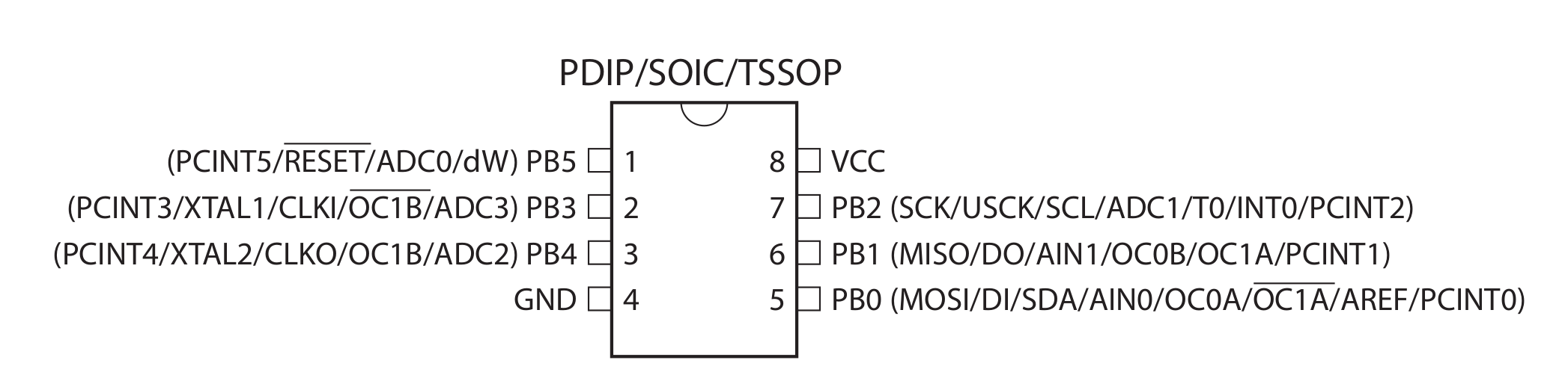
The ATtiny85 has 8 pins, of which 6 can be used as digital I/O (inputs or outputs). The I/O pins are named according to the port they belong to. In the following figure we see that the ATtiny85 pins are named PBx, where x is the number corresponding to the pin in the register (don't worry, we'll see more details below):
Each I/O pin can be used as input or output and also for other functions. For now we will only work with the pins functioning as GPIO (General Purpose Input/Output).
As shown in the image above, we have the following pins available on the ATtiny85:
PB0, PB1, PB2, PB3, PB4, PB5.
Some Particularities of the Franzininho DIY Circuit
The I/O pins are marked in yellow in the Franzininho DIY pinout.
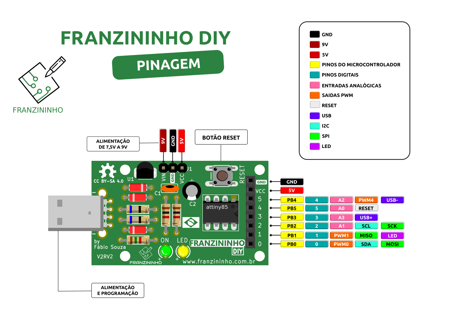
- Pin PB5 is configured as RESET on the Franzininho DIY, so we cannot use it as I/O.
- Pins PB3 and PB4 are used for the USB circuit, so we must use them with caution. These pins are generally used only as digital outputs.
- The yellow LED on the board is connected to pin PB1.
- Pins PB0 and PB2 have no circuits connected to them.
Registers Responsible for I/O Pins
To work with I/O pins on the ATtiny85 we have 3 registers:
- PORTB: Data register. Responsible for writing to the pins.
- DDRB: Pin direction register. Responsible for configuring pins to define whether they will be input or output.
- PINB: Port input register. Responsible for reading the pin state.
Note that all registers end with B. This means we are working with PORTB. If it were a microcontroller with more pins, we would have endings A, B, C, etc. Each port has a maximum of only 8 pins.
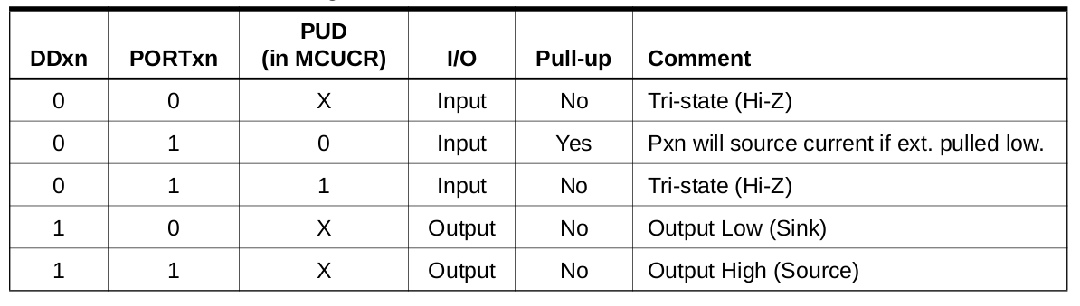
Section 10 of the ATtiny85 datasheet contains all the details for working with I/O. The following table, taken from the datasheet, shows the possible configurations for the pins:
The figure below shows the registers responsible for the PORTB I/O pins:
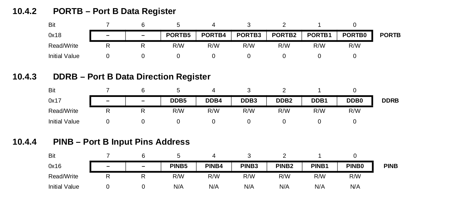
Note that each bit of the registers is responsible for a pin, indexed by the corresponding bit number. Therefore, if we want to use pin PB1 to drive the LED, we must configure the DDRB register as follows:
| 7 | 6 | 5 | 4 | 3 | 2 | 1 | 0 |
|---|---|---|---|---|---|---|---|
| - | - | 0 | 0 | 0 | 0 | 1 | 0 |
And to turn the LED on/off we must set 1 or 0 in the corresponding bit of PORTB.
Let's look at an example to make this clearer.
Code
#include <avr/io.h>
#include <util/delay.h>

#define F_CPU 16500000L        // Oscillator frequency, used for the delay function

int main(void)
{
  DDRB = 0b00000010;           // Configure pin PB1 as output (LED pin)

  while (1)
  {
      PORTB = 0b00000010;      // Turn on LED 1
      _delay_ms(250);          // Wait 250 ms
      PORTB = 0b00000000;      // Turn off LED 1
      _delay_ms(250);          // Wait 250 ms
  }

  return (0);
}
The example above blinks the LED at 250 ms intervals. The configuration of pin PB1 as output was done by setting bit 1 of DDRB to 1. To turn the LED on and off, bit 1 of PORTB was manipulated, alternating between 1 and 0.
Nice, right?
We can improve register bit manipulation using macros. Macros are routines that make our lives easier. I recommend reading this article to understand macros and the operations performed: https://www.embarcados.com.br/bits-em-linguagem-c/
Let's use the following macros:
#define setBit(value,bit) (value |= (1<<bit))
#define toggleBit(value,bit) (value ^= (1<<bit))
The names are self-explanatory, but let's see how to use them in the C program:
#include <avr/io.h>
#include <util/delay.h>

#define F_CPU 16500000L

// Macros
#define setBit(value,bit) (value |= (1 << bit))
#define toggleBit(value,bit) (value ^= (1 << bit))

int main(void)
{
    setBit(DDRB, PB1);          // Configure pin PB1 as output (LED pin)

    while (1)
    {
        toggleBit(PORTB, PB1);  // Toggle pin state
        _delay_ms(250);         // Wait 250 ms
    }

    return (0);
}
This way we manipulate only the desired bits without changing the values of others that may be used for other applications.
Challenge
Place another LED on pin PB0 and drive it alternately with pin PB1 — i.e., when the LED on PB0 is on, the LED on PB1 should be off and vice versa.
| Author | Fábio Souza |
|---|---|
| Date: | 24/04/2021 |